Key Sample Information :
-
Location : Rue J. Starcky
-
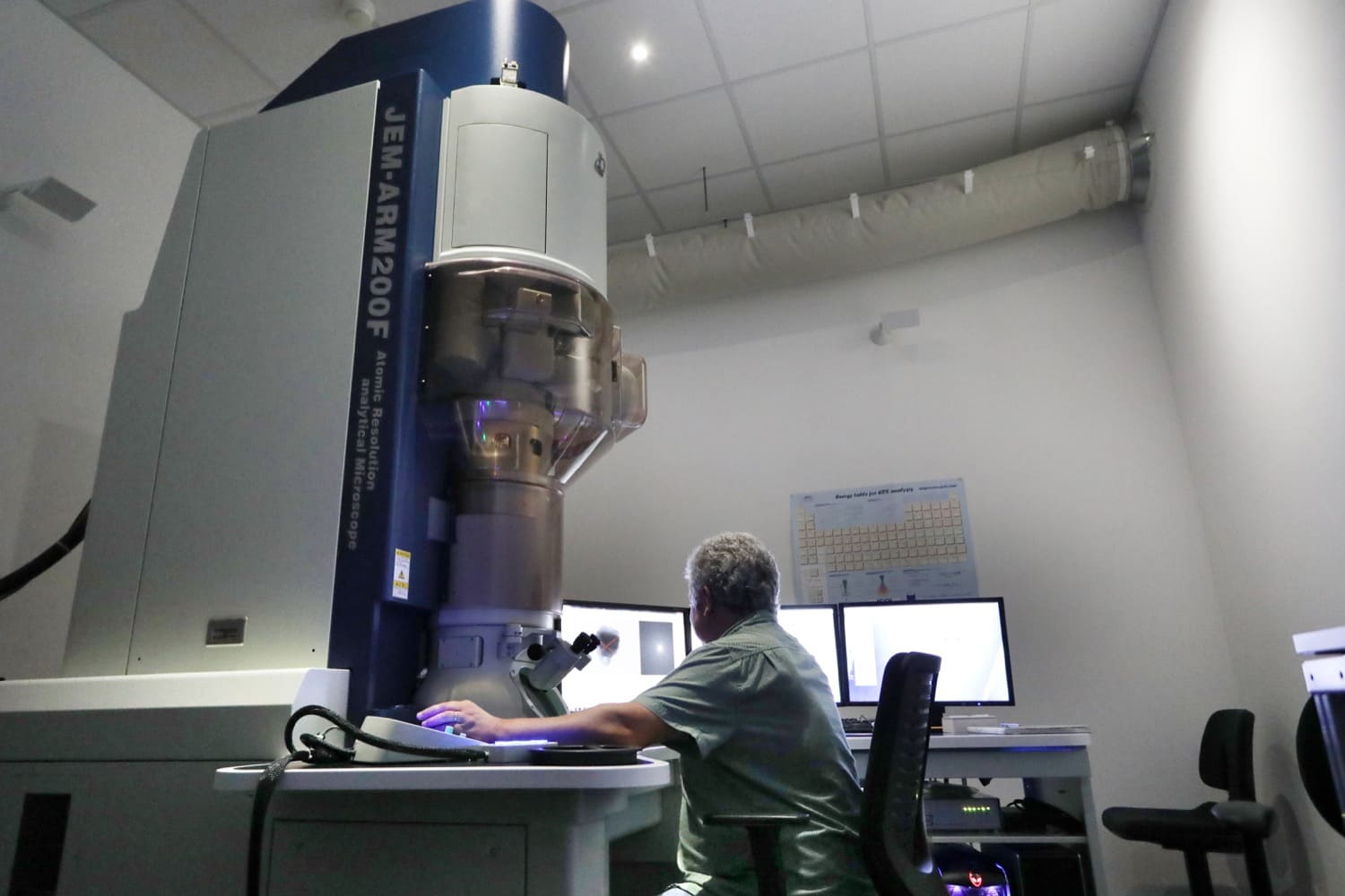
Electron Source : Cold Field Emission Gun (FEG) by Canon
-
Operating Mode : High vacuum
-
Acceleration Voltages : 80 kV or 200 kV
-
Configuration : TEM and STEM
-
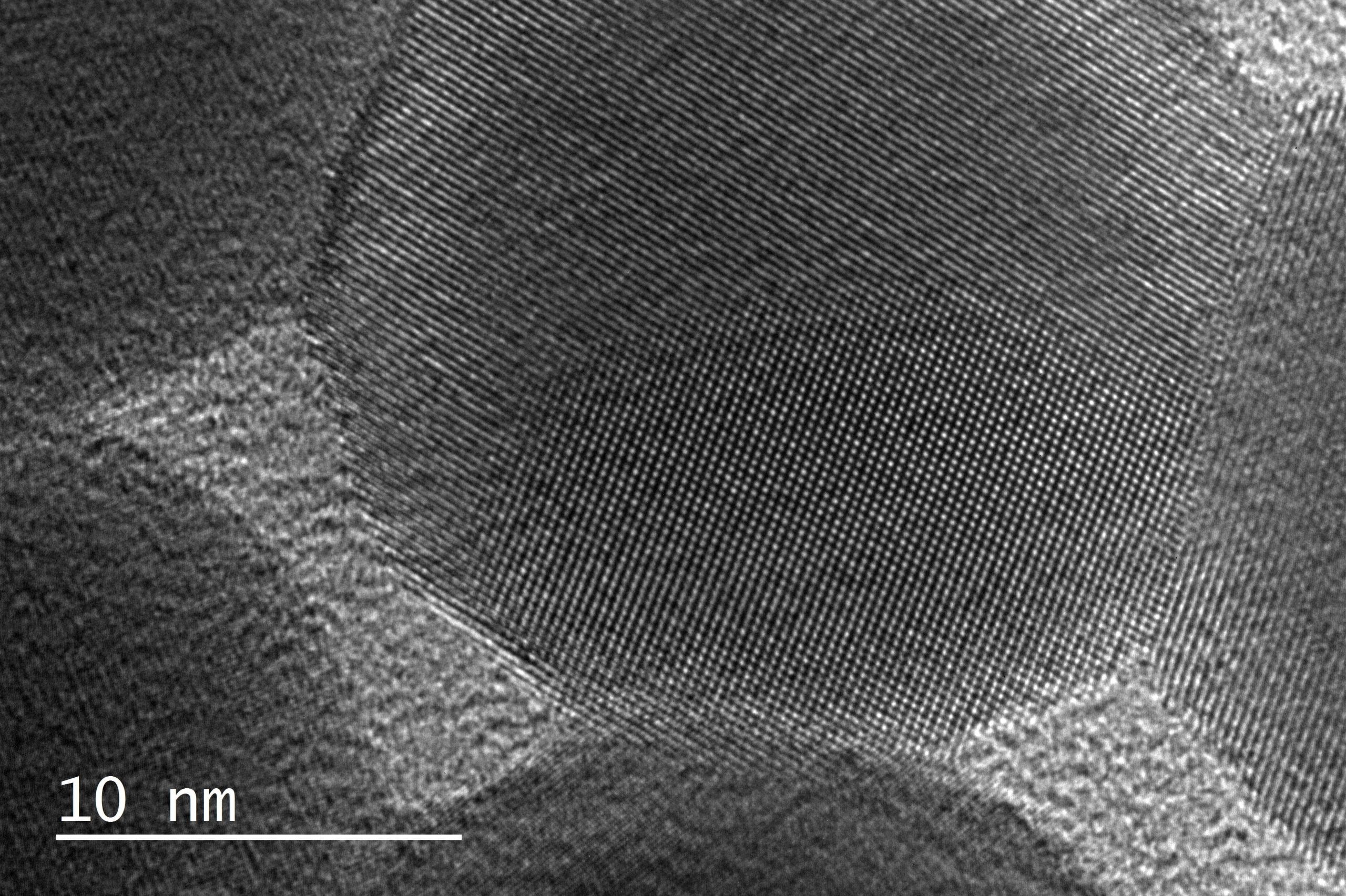
Spatial Resolution : 80 pm (lattice fringe mode)
-
Objective Lens Corrector : Yes
Sample Preparation
-
Samples must have a thickness of less than 100 nm, obtained through grinding, ultramicrotomy, or another suitable mineralization method.
Accessibility : Not available for self-service
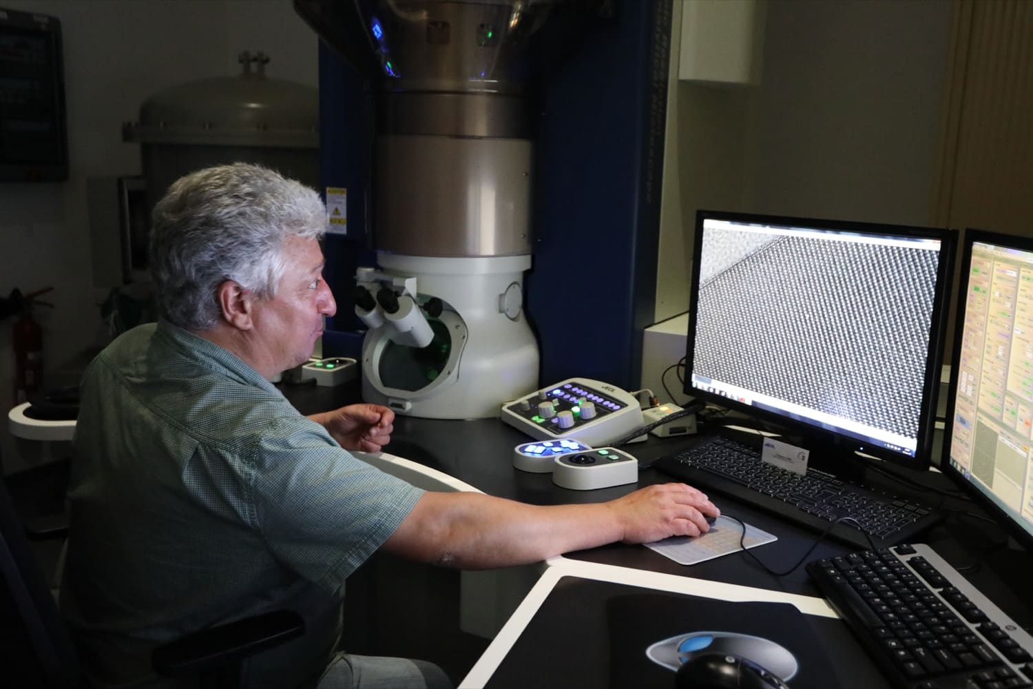
Transmission Electron Microscope – JEOL ARM200
A high-resolution TEM/STEM microscope dedicated to structural, chemical, and crystallographic analysis at the atomic scale.
What is it for ?
This microscope is intended for atomic-scale materials characterization :
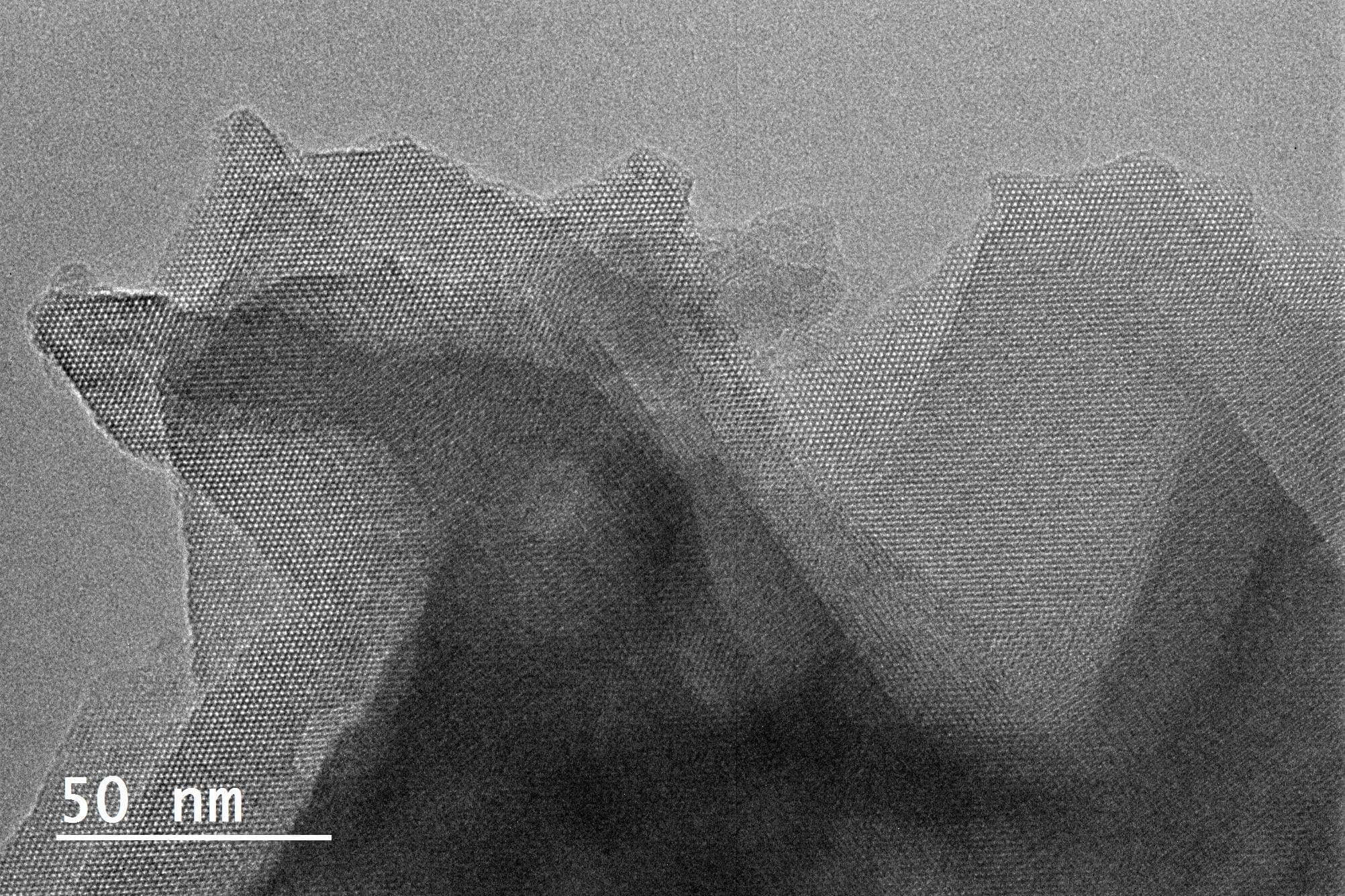
- imaging of crystal lattices,
- chemical mapping,
- fine structure or defect analysis,
- electron tomography
Fields of application :
- Nanomaterials and crystalline materials
- Semiconductors and thin films
- Ultra-thin biomaterials
- Catalysis, ceramics, functional polymers
- Materials science, chemistry, solid-state physics
Available Measurement Types
-
High-resolution TEM imaging : up to 80 picometers
-
STEM mode : for Z-contrast or high chemical sensitivity
-
EDX analysis :
-
Semi-quantitative
-
Detection starting from boron
-
Elemental mapping
-
Electron diffraction :
-
Determination of interplanar spacings
-
Crystalline phase analysis
-
Electron tomography :
-
3D reconstruction of nanoparticles or complex objects