AFM or Near Field Microscopy
The AFM platform characterizes materials and nanostructures by imaging at the nanometric and atomic scales.
Manager
Airoudj Aissam
Contacts : aissam.airoudj@uha.fr ou philippe.kunemann@uha.fr
Description
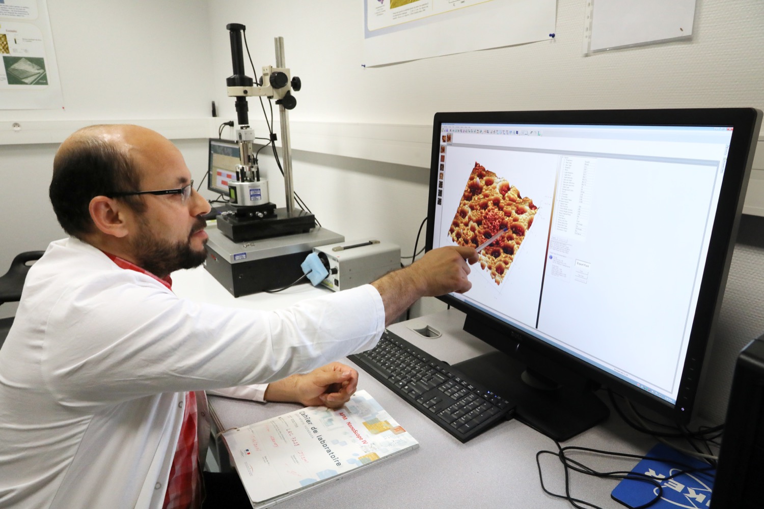
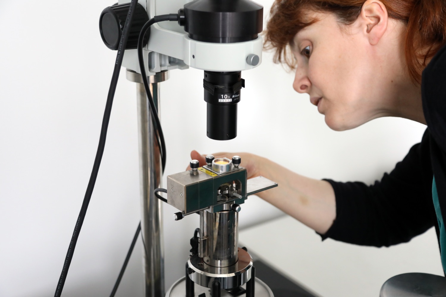
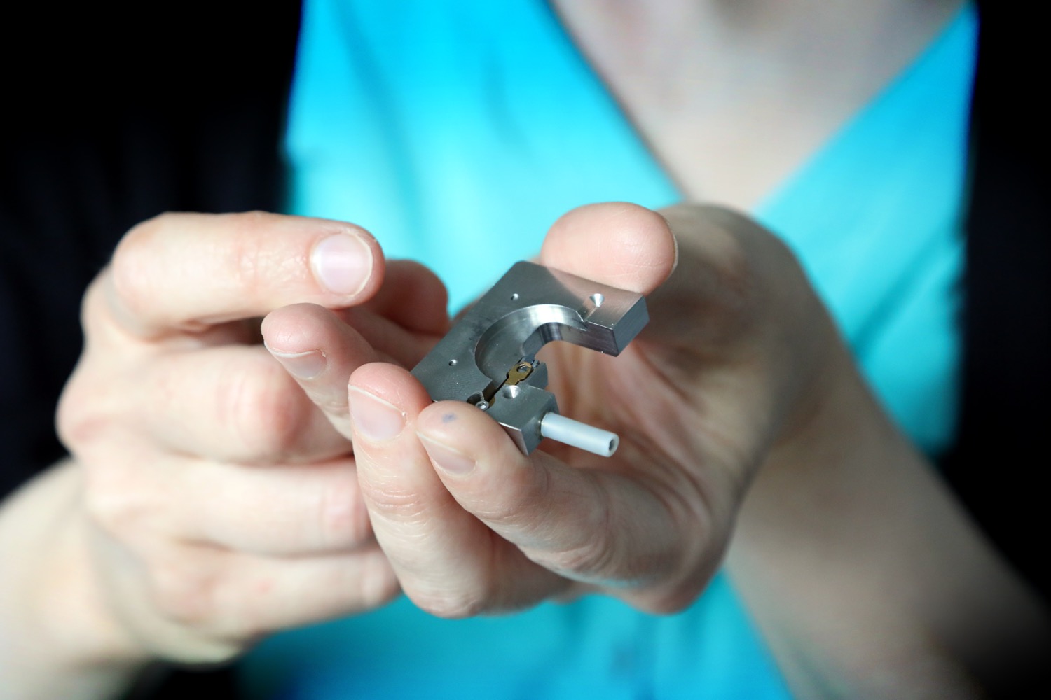
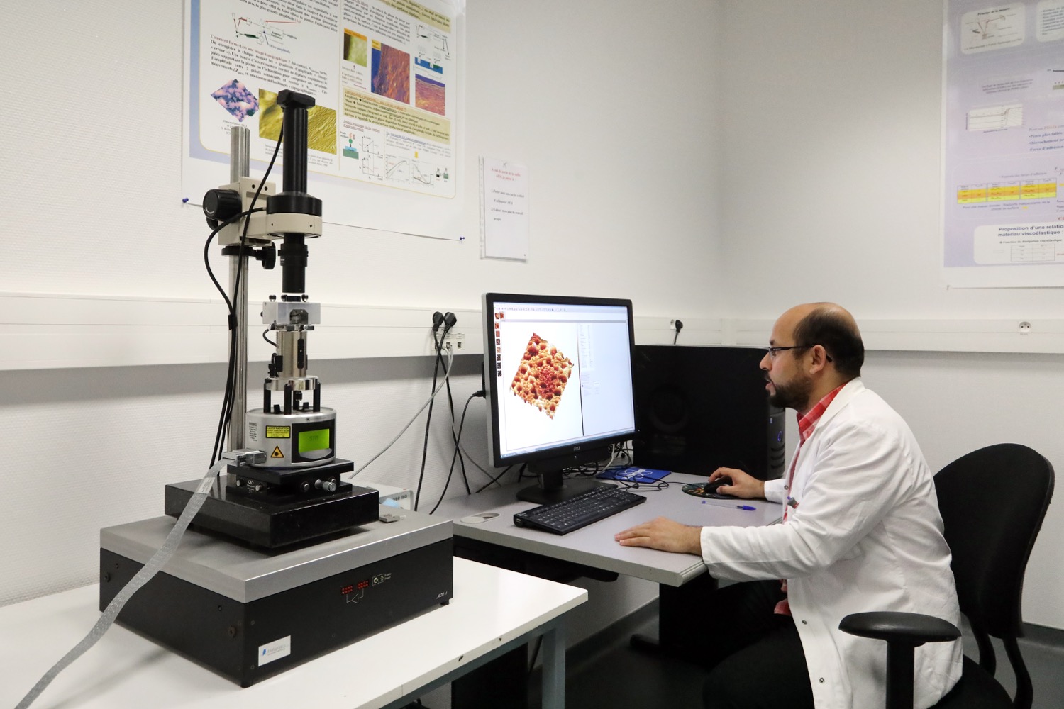
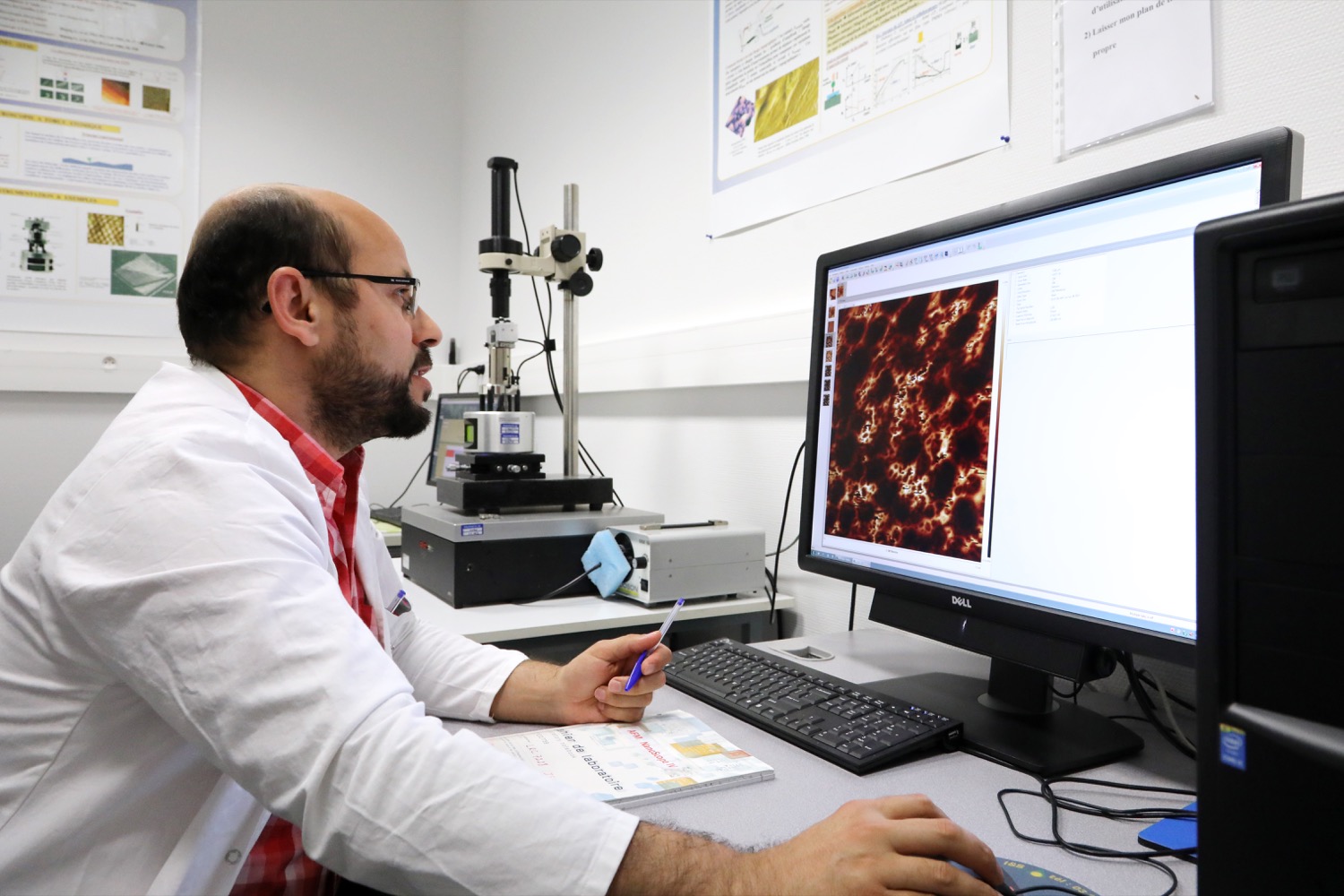
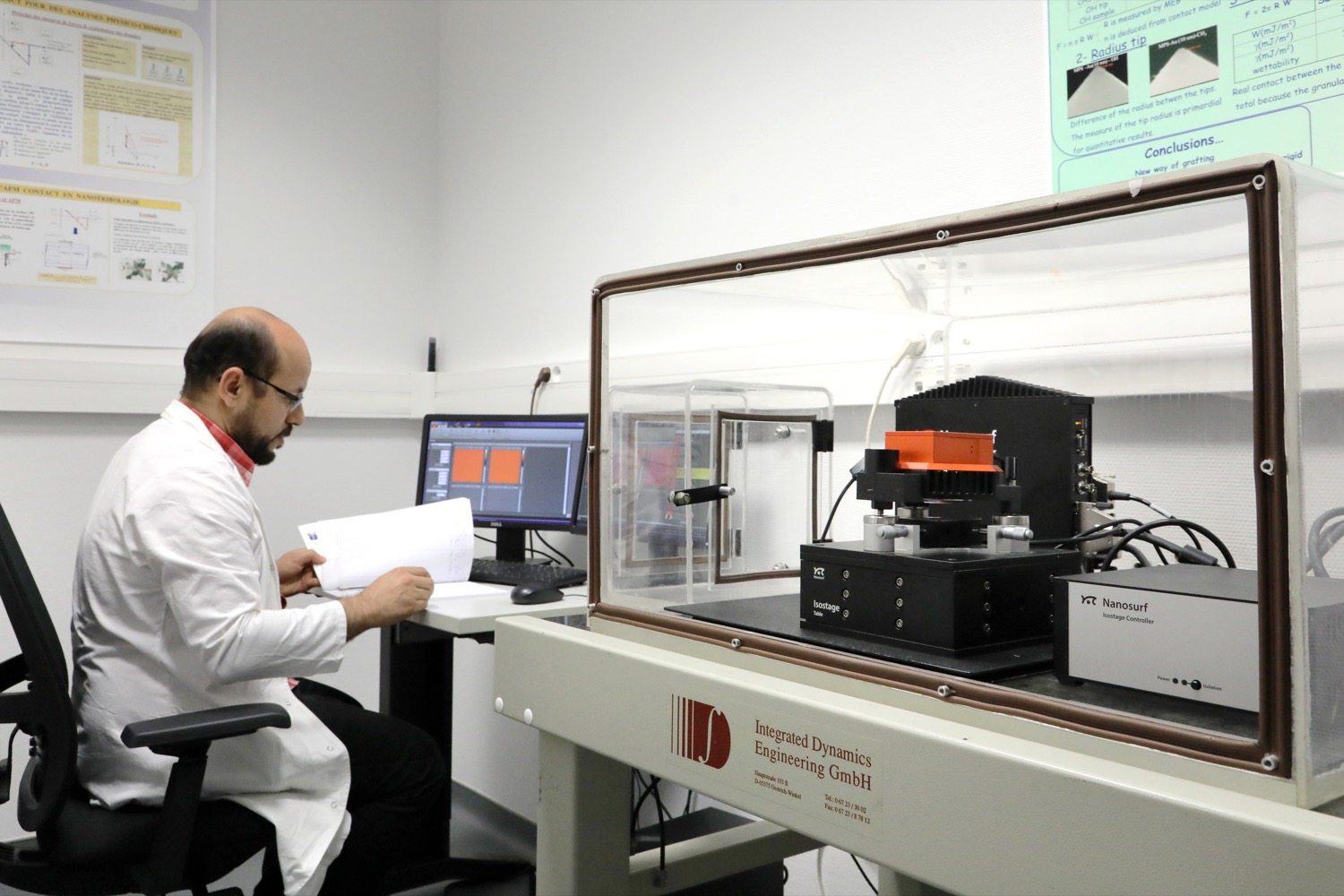
The AFM (Atomic Force Microscopy) platform at IS2M offers high-resolution imaging and nanoscale characterization of materials and surfaces. Based on local interactions between a sharp probe and the sample surface, this technique enables three-dimensional surface imaging with vertical resolutions down to the angstrom scale.
Beyond topographical mapping, the platform allows local measurement of physical (mechanical, electrical, magnetic) andchemical surface properties. It complements conventional microscopy techniques and addresses the increasing need for nanoscale surface analysis in research and development.
Available Measurements
- Topographical imaging (Contact, Tapping, PeakForce Tapping)
- Mechanical characterization (LFM, PeakForce QNM)
- Local conductivity and electrical properties (KPFM, EFM,TUNA, PeakForce TUNA, CAFM)
- Magnetic properties mapping (MFM, PeakForce MFM)
- Imaging in liquid, humid, or gas-controlled environments
- Scanning Tunneling Microscopy (STM)
Application Areas
- Functional materials and polymers
- Surface and interface science
- Nanotechnology and electronic devices
- Coatings and surface treatments
- Biomaterials and biological systems
- Materials science, chemistry, physics, and surface engineering
Accepted Sample Types
- Thin films and coated surfaces
- Bulk materials with smooth or polished surfaces
- Nanoparticles deposited on substrates
- Functionalized or treated surfaces
- Biological samples (under specific conditions)
- Samples compatible with liquid, gas, or controlled-temperature environments
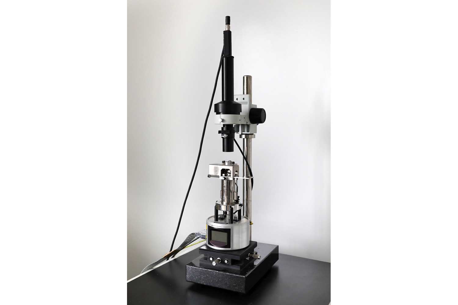
Equipement


IS2M
Bâtiment CNRS
15, rue Jean Starcky - BP 2488
68057 Mulhouse cedex
Bâtiment IRJBD
3 bis, rue Alfred Werner
68093 Mulhouse cedex
tel: (+33)3 89 60 87 00
fax: (+33)3 89 60 87 99
