Electron Microscopy
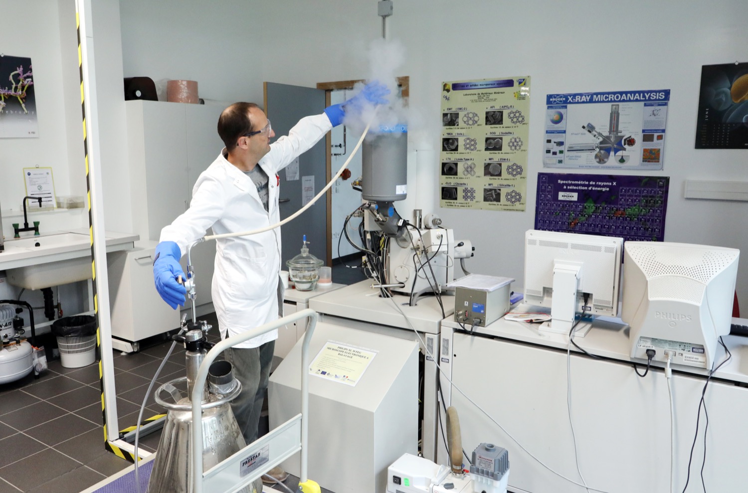
Electron microscopy allows the observation of all types of materials from the nano to the macro scale. The information obtained provides insights into surface morphology and chemistry, as well as internal organization and chemicalcomposition.
Manager
Vidal Loïc
Contacts : loic.vidal@uha.fr ou ludovic.josien@uha.fr
Description
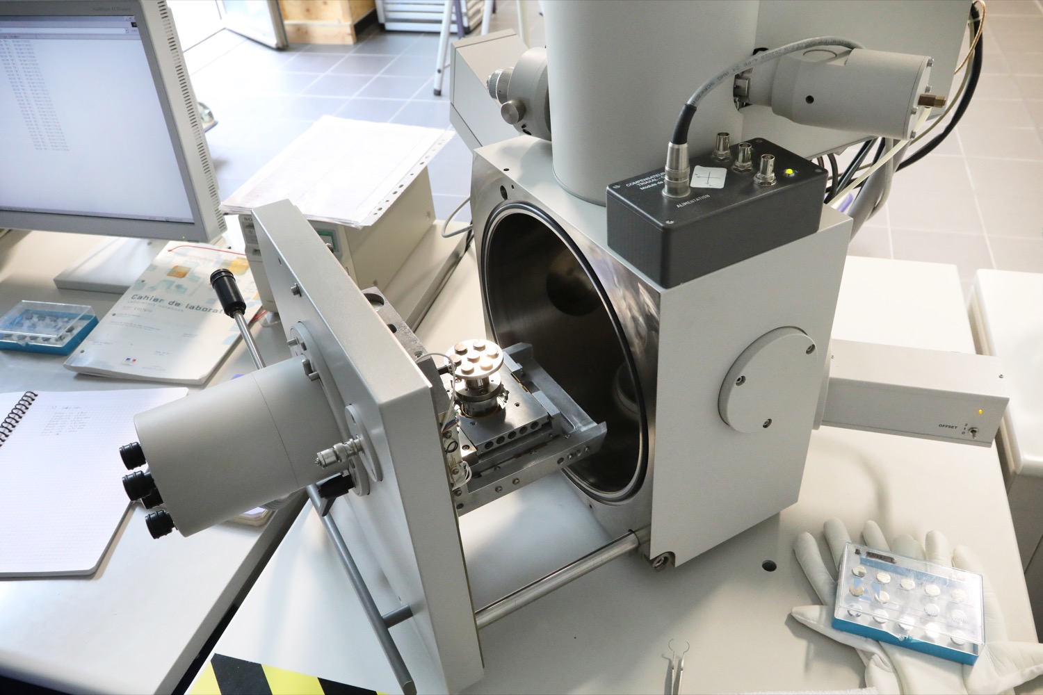
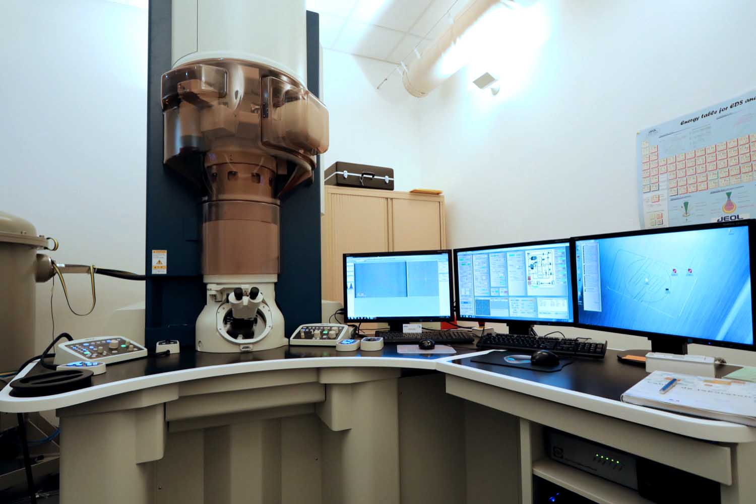
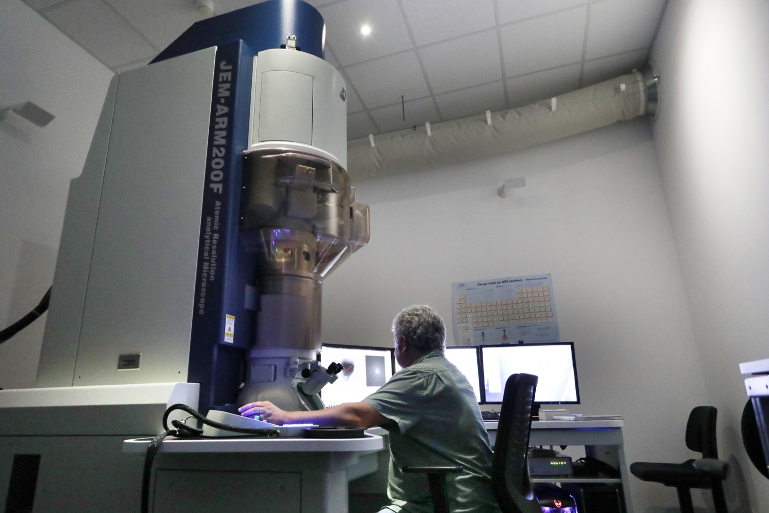
The electron microscopy platform allows for the observation and analysis of all types of materials, from the nanometerscale to the macroscopic scale. With its advanced equipment (scanning electron microscopes – SEM – and transmission electron microscopes – TEM), it provides detailed information about the morphology, internal organization, crystallographic structure, and chemical composition of samples.
This platform is a versatile tool used across many fields of research and innovation, particularly for the characterization of complex materials, fine structures, or critical interfaces.
Available Measurements
-
High-resolution imaging (down to atomic scale with TEM)
-
Topographical imaging (SEM)
-
Elemental mapping via EDX spectroscopy
-
Phase/crystallinity analysis by electron diffraction
-
Transmission and scanning imaging modes
-
2D/3D imaging, layer thickness measurements
Application Areas
-
Materials science (polymers, ceramics, composites, metals, alloys…)
-
Nanotechnologies and nanostructured objects
-
Characterization of porous and functional materials
-
Biomaterials and biological objects
-
Microelectronics and surface engineering
-
Environmental studies (fine particles, solid pollutants…)
Accepted Sample Types
-
Solid materials (organic, inorganic, hybrid)
-
Powders, fibers, thin films
-
Porous materials, polymers, carbons
-
Biological samples (prepared according to protocol)
-
Nanostructured or microstructured objects
Descriptif technique


IS2M
Bâtiment CNRS
15, rue Jean Starcky - BP 2488
68057 Mulhouse cedex
Bâtiment IRJBD
3 bis, rue Alfred Werner
68093 Mulhouse cedex
tel: (+33)3 89 60 87 00
fax: (+33)3 89 60 87 99
