

Equipments
Equipements
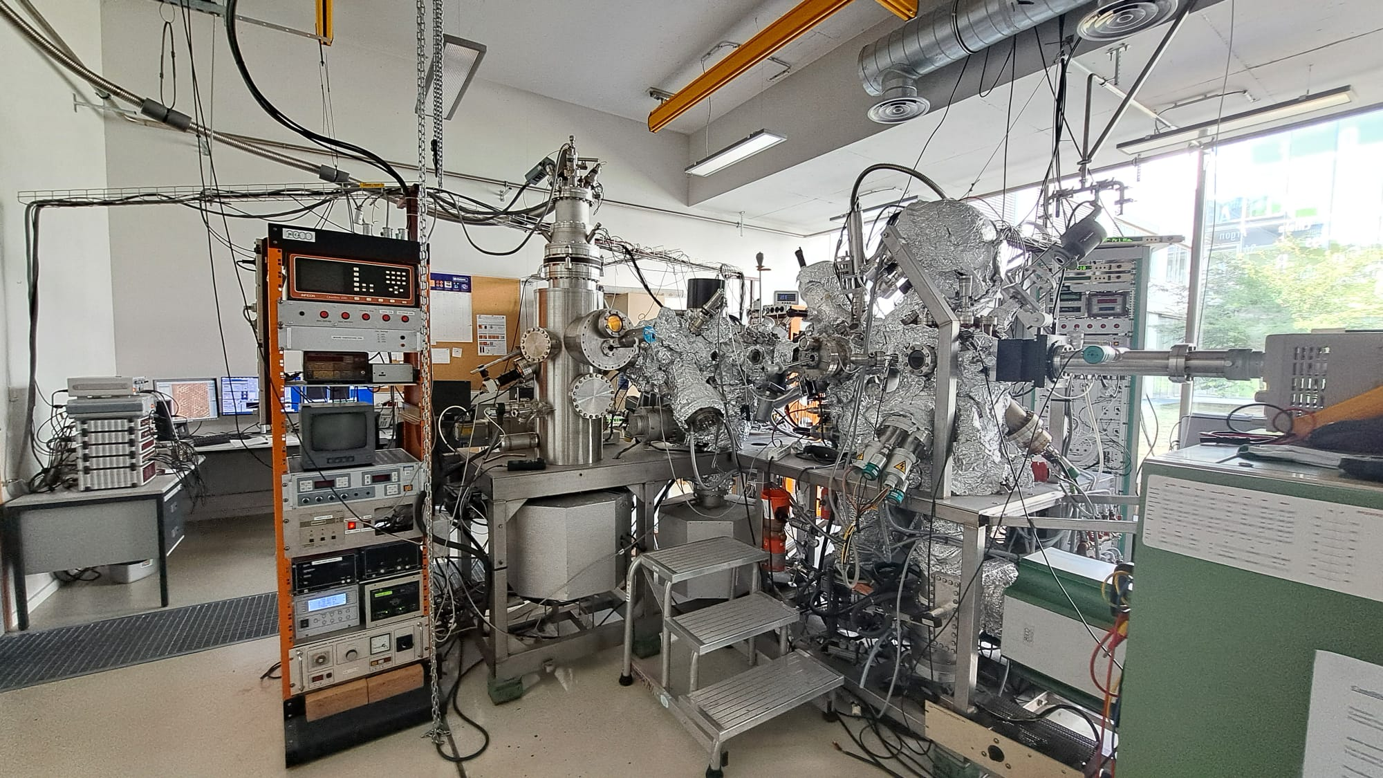
Ultra high Vacuum Platform
The ultra-high vacuum (UHV) platform brings together a comprehensive suite of complementary surface analysis techniques, including Scanning Tunneling Microscopy (STM), photoemission spectroscopy (XPS, UPS, and ARPES), and electron diffraction (LEED and XPD). Combined with a variety of organic and inorganic thin-film deposition capabilities, this platform enables structural and electronic characterization of surfaces from the atomic to the macroscopic scale. It provides a unique environment for investigating the morphology, atomic structure, chemical composition, and electronic properties of materials with both local and global sensitivity.
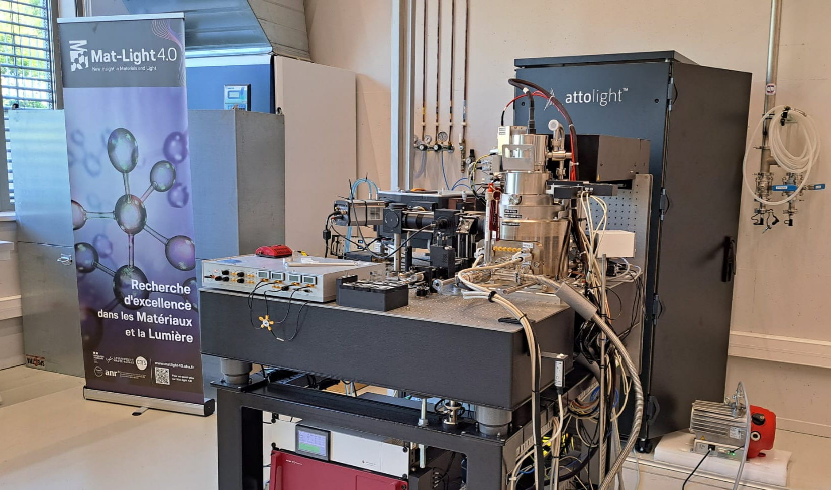
Correlative Microscopy Platform
Our research group manages a state-of-the-art correlative microscope as part of the Mat-Light 4.0 project. The Allalin microscope (Attolight) is a state-of-the-art correlative microscopy platform that integrates scanning electron microscopy (SEM), cathodoluminescence (CL), photoluminescence (PL), Raman spectroscopy, two- terminal electrical transport measurements, as well as hyperspectral imaging and time-resolved spectroscopy. This unique instrument enables the nanoscale mapping of the structural, optical, and electronic properties of materials over a wide temperature range, from cryogenic conditions to room temperature. By directly correlating morphology, composition, and functional properties, the Allalin microscope provides unprecedented insights into semiconductors, quantum materials, nanostructures, and optoelectronic devices, making it a powerful platform for investigating charge carrier dynamics, recombination mechanisms, and local material heterogeneities.
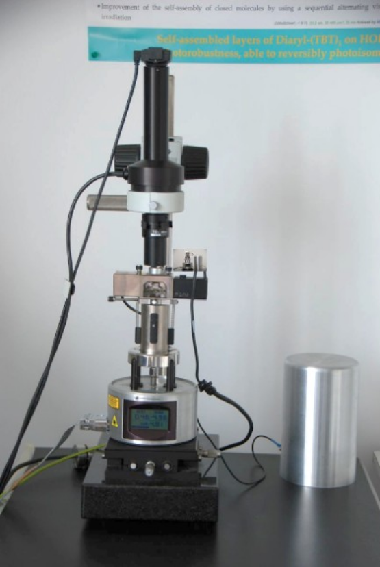
Scanning-Probe Platform
Atomic Force Microscopy (AFM), Conductive AFM (C-AFM), Kelvin Probe Force Microscopy (KPFM), and Scanning Tunneling Microscopy (STM) at the solid–liquid interface provides complementary nanoscale characterization techniques for investigating the surface properties of a wide range of materials. These techniques enable high-resolution mapping of surface topography, local electrical conductivity, and work function, while STM offers atomic-scale imaging and electronic characterization at the solid–liquid interface. Together, they provide powerful tools for studying metals, semiconductors, molecular materials, and nanostructures.
IS2M
Bâtiment CNRS
15, rue Jean Starcky - BP 2488
68057 Mulhouse cedex
Bâtiment IRJBD
3 bis, rue Alfred Werner
68093 Mulhouse cedex
tel: (+33)3 89 60 87 00
fax: (+33)3 89 60 87 99
