

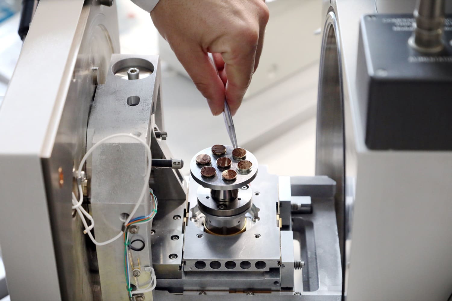
Key Information:
- Location: Rue J. Starcky
- Electron source: Tungsten filament
- Operating modes:
- High vacuum and low vacuum (partial vacuum): Allows observation of both conductive and non-conductive samples (without complex sample preparation).
- Adjustable accelerating voltage: Adaptable to different types of samples to optimize contrast and resolution.
- Accelerating voltage: Adjustable from 0.3 kV to 30 kV.
- Resolution:
- 3.0 nm at 30 kV (high-vacuum mode)
- 4.0 nm (low-vacuum mode).
- Accessibility: Available for self-service use after training.
Scanning Electron Microscope – JEOL JSM-IT210
A scanning electron microscope dedicated to the observation and characterization of the morphology, microstructure, and chemical composition of different types of materials.
What can it be used for?
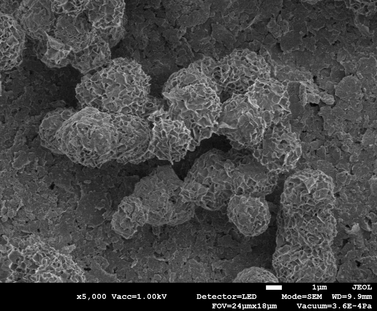
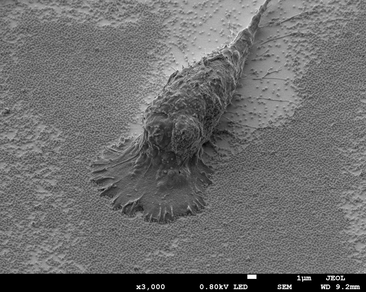
This microscope enables materials to be characterized at the micro- and nanoscale in order to study:
- surface morphology and topography;
- particle size, shape, and distribution;
- material microstructure;
- defects, cracks, and heterogeneities;
- surface organization and structure.
Application Areas:
- Polymers and composite materials;
- Nanomaterials and particles;
- Metals and alloys;
- Ceramics and mineral materials;
- Porous and carbon-based materials;
- Fibers, coatings, and thin films;
- Biomaterials;
- Materials science and quality control.
Types of Measurements Available:
- Scanning Electron Microscopy (SEM) imaging:
- observation of morphology;
- study of surface topography;
- characterization of microstructure.
- Imaging at different magnifications:
- observation of structures ranging from the micrometer to the nanometer scale.
- Chemical composition analysis:
- elemental identification;
- semi-quantitative analyses;
- chemical mapping.